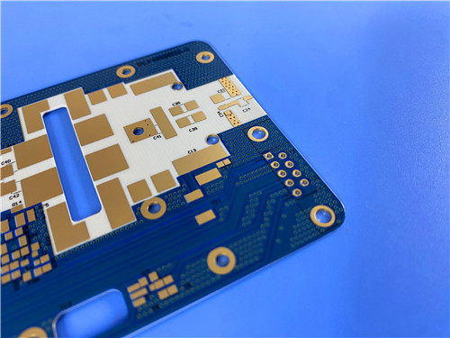
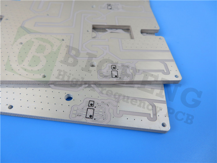
Taconic RF-60A 2-Layer PCB for Advanced RF Applications1.Product Overview Taconic's RF-60A organic-ceramic laminate combines woven glass reinforcement with proprietary ceramic technology to deliver exceptional performance for demanding RF applications. This 2-layer PCB material features outstanding dimensional stability (CTE 9/8/69 ppm/°C), ultra-low moisture absorption (0.02%), and excellent thermal reliability for consistent high-frequency operation. 2.Key Technical Specifications Dielectric Constant: 6.15 @10GHz 3.PCB Construction Specifications
4.PCB Stackup: 2-layer rigid PCB Copper_layer_1 - 35 μm 5.PCB Statistics: Components: 9 6.Performance Advantages Enhanced dimensional stability 7.Typical Applications 5G power amplifiers 8.Quality Assurance IPC-Class 2 compliant This high-performance RF-60A PCB solution delivers reliable signal integrity for mission-critical wireless applications while maintaining cost efficiency for volume production. |
Get a Quick Quote
Fill in the form below and our engineers will reply within 24 hours with technical specifications and pricing for Taconic RF-60A 2-Layer PCB for Advanced RF Applications.
.jpg)
.jpg)
.jpg)
.jpg)
.jpg)
.jpg)
